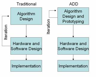
Introduction
Certain algorithms do not run efficiently or effectively on the processors inside most consumer computers. Consumer processors are optimized to be very multi-purpose. Among their many functions, they can run operating systems, interface with peripheral devices and control the monitor. A large amount of overhead including memory and control logic is required to handle so many functions.
Algorithms that require the use of large amounts of data, include feedback (either in the form of filters or using the same data multiple times), and necessitate fast arithmetic are not well suited to be run on consumer processors. Instead, these types of algorithms must be run on a more optimized, streamlined system. Often such algorithms must run in real-time, which further emphasizes the need for fast, clean computation.
There is a certain type of chip, namely a Digital Signal Processor (DSP), that is specifically designed for these types of algorithms.
^ TOPHistory
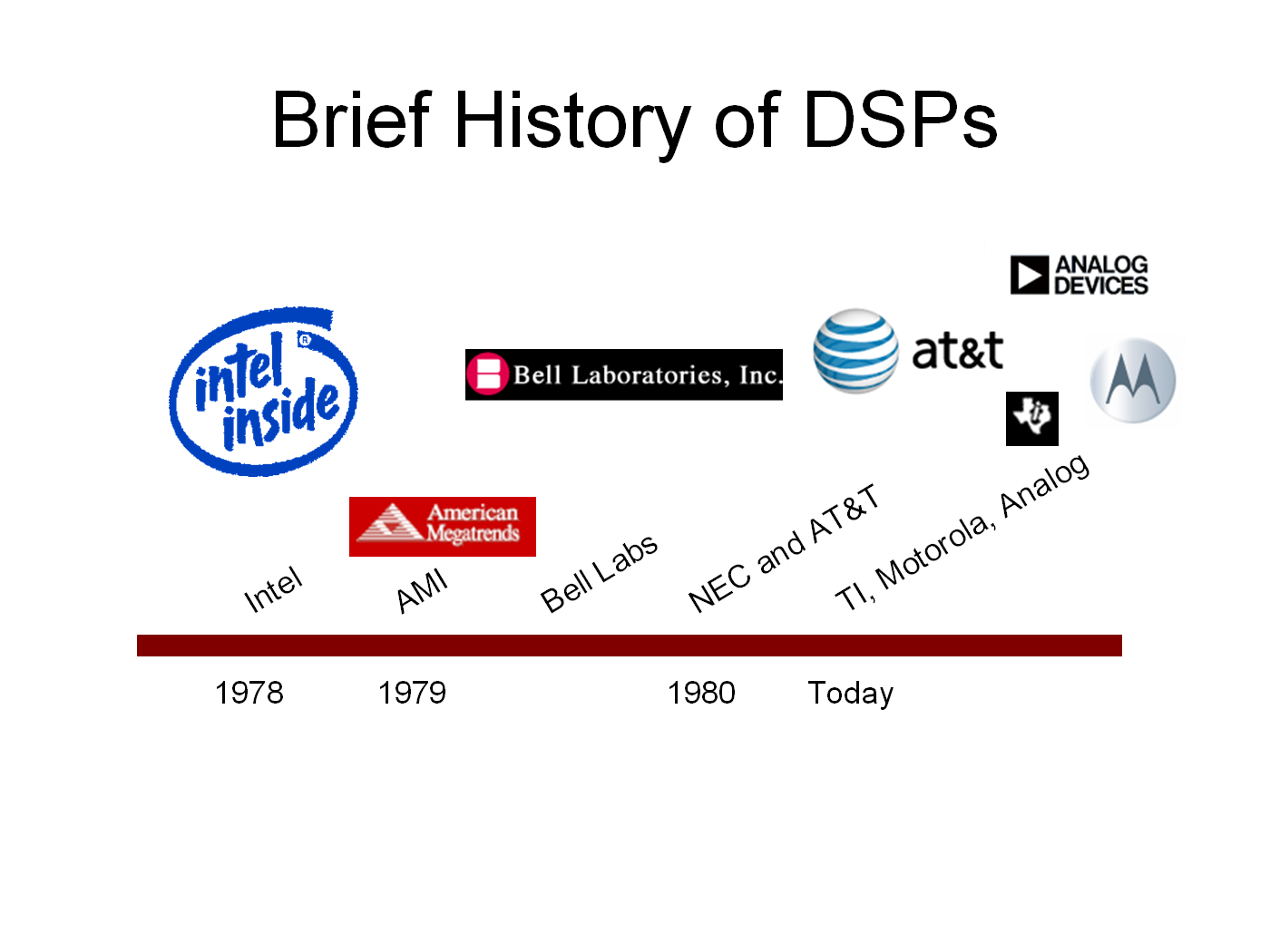
DSPs were invented in the late 1970s. In 1978, Intel created a chip with an on-chip analog-to-digital converter and digital-to-analog converter (DAC) with an internal signal processor. However, the chip had no hardware multiplier and ultimately failed.
In 1979, American Megatrends created a similar device, but framed it as a microprocessor peripheral. The chip was host-initialized, and also ultimately failed.
In 1980, Bell Laboratories created the first single-chip DSP. In 1981, NEC and AT&T followed suit, creating their own DSPs. These telecom companies were derived from research the telecom companies had been doing for Public Switched Telephone Networks (PSTN).
Today, there are three major suppliers of DSPs: Texas Instruments, Analog Devices and Motorola.
^ TOPAnalog Devices Blackfin
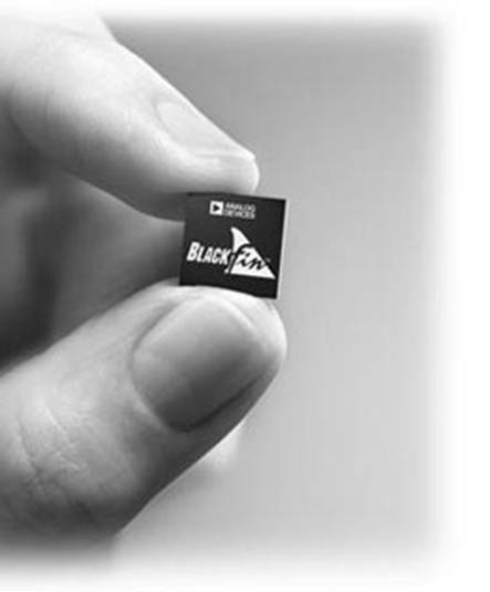
Most DSPs share certain functionalities. The implementation is often different, but the end results are similar. The 'Blackfin' DSP from Analog Devices will be explored as an example. It can be assumed that other DSPs, while not identical to the Blackfin, will look similar.
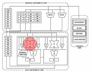
The Blackfin has a number of architectural components that assist in the execution of the types of algorithms mentioned above.
^ TOPFast Mac
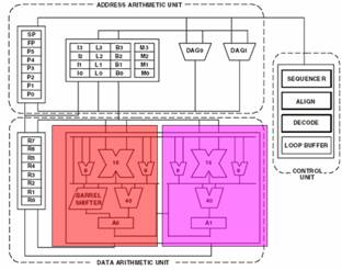
TThe multiply-accumulate operation is at the heart of most signal processing operations. It is the basis for convolution, which is the basis for many higher-level functions. The Blackfin has a 16-bit multiplier and a 40-bit accumulator. It is true that multiplying two 16-bit numbers will never give more than a 32-bit output. The extra 8 bits, however, are not superfluous - they exist so when the accumulator adds up the products of the multiplier, it has an extra 8 bits to work with before it overflows.
Fast MACs are very important for DSPs. The faster the DSP can execute a MAC, the more data can be processed. The Blackfin can execute 1.2GMACs at 600MHz, more than twice that of its closest competition.
^ TOPParallelism
Parallelism is another important property of DSPs. Often, the same operation must be done many times on multiple sets of data. Having twice the amount of hardware doubles the rate at which data can be processed.
The Blackfin has two MAC units, as described above. It also has four 8-bit Arithmetic Logic Units (ALUs) devoted solely to video processing. Every clock cycle, each video ALU can output a 4-pixel difference frame. That is, the ALU will compare four pixels from one image and the four pixels in the same location in another image. The output is a measure of how similar the two images are. This is very useful for applications such as stereo vision.
^ TOPPipelines
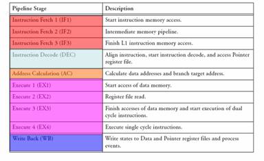
Pipelining is a method used to keep all sections of the ALU constantly computing. Pipelining is explained here and here (link to external references). The Blackfin uses a 10-stage pipeline. The first three stages are Instruction Fetch stages, where the ALU reads an instruction from memory. The fourth stage is the Instruction Decode phase, where the ALU determines what the instruction is telling it to do and sets itself up accordingly. The fifth stages is the Address Calculation stage, where the ALU calculates addresses for data access and branch targets.
The Blackfin then has four Execute phases, where it implements the functions that the instruction specified. Finally, the Write Back phase occurs, in which the ALU stores any required output.
^ TOPStorage
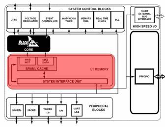
The hardest task facing a DSP designer is not to make the ALU fast, but to send it data fast enough to keep it busy. Since disk access takes a very long time, the Blackfin has a large amount of L1 cache memory right next to the core. The memory is connected to the core via 64-bit high-speed buses
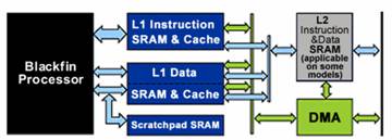
The Blackfin, like many other DSPs these days, uses a modified form of the Harvard architecture. There are separate L1 caches for instructions and data, each with their own separate buses to the core. This ensures that instructions are not tying up valuable bandwidth on the data lines, allowing data to flow as quickly as possible.
The instruction bus is 64-bits wide. Since the Blackfin uses a variable-length instruction set (instructions can be either 16 bits or 32 bits), two to four instructions can be fetched at once. There are two data buses, each 32 bits wide with corresponding 32-bit address lines.
^ TOPExternal Interface
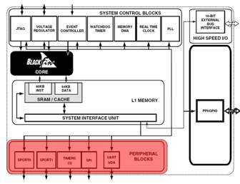
It would not be very useful to have a chip that can process data really fast if you couldn't give it data or take results back. So, the Blackfin has a number of external interfaces. There is a 100Mbps serial port, as well as a high-speed parallel port capable of moving digital video on and off the chip. There are memory interfaces as well, for SDRAM, Flash, SRAM, etc.
^ TOPDual Core
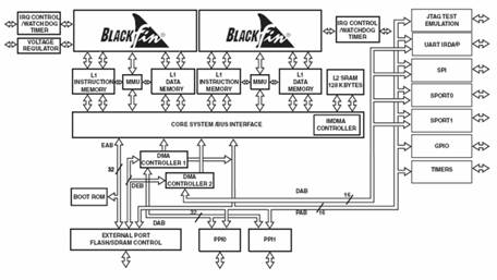
The Blackfin comes in a single core or a dual core model. There are various advantages to using a dual core model instead of a single core.
For instance, if two software teams develop two separate pieces of code, it's a non-trivial task to merge the two programs in such a way that they can peacefully coexist on a single core. With a dual core DSP, each program can run on a separate core.
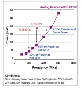
Even if only a single program exists, running half of it on one core and half on the other can be advantageous. By using twice the hardware, the clock rate can be halved without affecting data throughput. A slower clock rate translates directly to lower power consumption, as shown in the following chart. The Blackfin contains an on-chip Phase-Lock Loop (PLL) to control the clock frequency and voltage.
Some applications require real-time data processing and also some sort of control structure, such as a GUI. With a dual-core DSP, these functions can be delegated to separate cores. This ensures that the GUI doesn't interfere with the real-time data processing.
^ TOPResearch
Current research into DSPs is focused in a number of areas, including modeling, design and DSP-FPGA porting.