Architecture
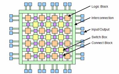
Regardless of the type of FPGA or the manufacturer, FPGAs have a very flexible architecture. A generalized architecture for an FPGA is shown below:
 ^ TOP
^ TOP
Logic Block
A logic block is the basic functional unit of the FPGA. From one FPGA to another, logic blocks may vary in many ways including size, functionality, and number of inputs and outputs. All logic blocks consist of some combination of these basic functional units:
- Transistor pairs
- Basic small gates (such as two-input NAND's or exclusive-OR's)
- Multiplexers
- Look-up tables (LUT's)
- Wide-fanin AND-OR structures
Depending on the type of logic blocks used, the FPGA will either be classified as fine grained or coarse grained. Fine grained FPGAs often consist of just a couple transistors, a couple logic gates, or a simple 3-input LUT, whereas a course grained FPGA has logic blocks that consist of more complex functional units, such as a 4-input LUT. Of course there are trade offs between fine grained and coarse grained FPGAs. The complexity of coarse grained FPGAs generally allow them to be able to perform harder functions, but the flip side of that is it is often difficult to fully take advantage of all the potential functionality in a coarse grained FPGA, so there is a high potential for space to be wasted and underutilized. While fine grained FPGAs can achieve a higher block density, there tend to be more interconnections required between the logic blocks, often consuming a significant amount of space in the design.
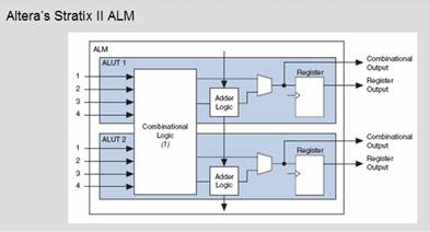
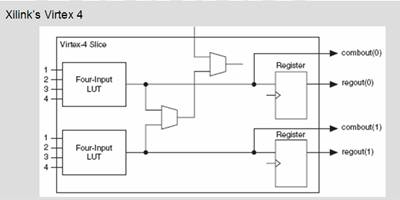
Two examples of logic blocks are the Actel's Stratix II, and Xilinx's Virtex 4. The basic logic block of the Stratix II, which Actel calls the Adaptive Logic Module (ALM), consists of two 4-input LUTs, two adders, and two registers. The Virtex 4 has a similar logic block structure; it is made up of two 4-input LUTs, multiplexers, carry logic, and two registers. The Stratix II can be configured to act as one larger LUT with up to 7 inputs, whereas to get this functionality in the Virtex 4, a couple logic blocks must be cascaded to use in series to achieve this functionality.
 ^ TOP
^ TOP
Interconnection
The interconnected components of the FPGA make up its routing. The various routing wires may be of different lengths, and carry signals in all directions throughout the FPGA. There are tradeoffs in determining the number of routing paths in a design as for an FPGA with a very limited number of routing paths, there may not be an adequate number of paths to move signals between all of the logic blocks. Likewise, in a design with too many routing paths not all of the paths will be utilized so space is wasted.
Switch boxes are used to enable a routing path to change direction, and connect blocks are used to control the flow of signals for a given direction. Tradeoffs exist in determining the lengths that the routing paths should be as longer paths that are not obstructed by switch boxes and connect blocks may transmit a signal faster, though clearly shorter routing paths are needed to quickly move signals from one logic block to a neighboring one.
^ TOP
The input/output ports on an FPGA logic block are used to provide the logic block with information for a given calculation, and then transport the result of that calculation back out of the logic block. The incoming and outgoing signals from the logic block may then be carried to other locations on the FPGA by means of routing paths so that more computations may be performed.
^ TOP
Connect Block
Connect blocks pass signals from one routing path to another, connecting routing paths of various lengths. Connecting blocks provide multiplexers with input signals to select from, before passing on signals to logic blocks.
^ TOP
Switch Box
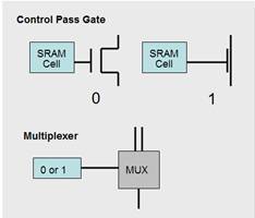
Switch boxes are used to enable a routing path to change direction; they occur at intersections of routing paths. There are three main types of switch boxes: SRAM, antifuse, and EPROM.
SRAM
Static Random Access Memory (SRAM) is commonly used in switch boxes. Whether or not a certain signal is passed through the switch box is controlled by the state of the SRAM bit, which can be either 0 or 1. When the value 1 is stored in the SRAM cell, there is low resistance between two wires so the SRAM cell functions as a closed switch. Alternatively, when a 0 is stored in the SRAM cell there is high resistance between the two transistor wires so the cell functions as an open switch.
Switch boxes can also be controlled by a multiplexer, which functions much the same way as an SRAM cell. A signal is allowed to pass through depending on the state of the multiplexer.
There are a number of advantages and disadvantages to each of these types of switch boxes. For SRAM, the switches are volatile so reprogramming of the switches is required every time the FPGA is powered on. Because this reprogramming is required, external memory is needed to provide this reprogramming data, adding to the hardware required and hence the cost, and to the space needed to support this additional hardware. On the other hand, the easily reprogrammable chip can be advantageous for development purposes.
 Antifuse
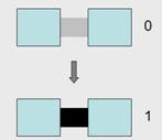
By default, antifuse switches are set to 0 as there is a high resistance path between two terminals. When a high voltage (often 11 to 20 V, depending on the specific chip) is applied across the terminals, a lower resistance path is created so the switch is then set to 1.
Antifuse switches have the disadvantages of not being reprogrammable and requiring extra circuitry to provide the switches with high voltage to set their state. Antifuse switches are, on the other hand, quite small, have very low series resistance, and low parasitic capacitance, making them an ideal choice if you do not plan on needing to reprogram your FPGA.
Antifuse
By default, antifuse switches are set to 0 as there is a high resistance path between two terminals. When a high voltage (often 11 to 20 V, depending on the specific chip) is applied across the terminals, a lower resistance path is created so the switch is then set to 1.
Antifuse switches have the disadvantages of not being reprogrammable and requiring extra circuitry to provide the switches with high voltage to set their state. Antifuse switches are, on the other hand, quite small, have very low series resistance, and low parasitic capacitance, making them an ideal choice if you do not plan on needing to reprogram your FPGA.
 EPROM
Erasable Programmable Read Only Memory (EPROM) FPGAs have two transistors at each switch box location: the Control Gate and the Floating Gate, separated from each other by the thin oxide layer. The charge of the oxide layer determines whether or not the high voltage from the Floating Gate will be passed through the Control Gate to the Word Line or to ground. When the Word Line has a high voltage the value is 1, and when it is at a low voltage the value is 0.
EPROM
Erasable Programmable Read Only Memory (EPROM) FPGAs have two transistors at each switch box location: the Control Gate and the Floating Gate, separated from each other by the thin oxide layer. The charge of the oxide layer determines whether or not the high voltage from the Floating Gate will be passed through the Control Gate to the Word Line or to ground. When the Word Line has a high voltage the value is 1, and when it is at a low voltage the value is 0.
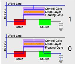 Disadvantages of EPROM switch boxes include that the transistors have high resistance, consume a lot of power, and require exposure to UV light to be reprogrammed. They do have a number of advantages as they do not require external memory to retain their state (as SRAM requires) and being reprogrammable makes them valuable during development and testing (unlike antifuse).
^ TOP
Disadvantages of EPROM switch boxes include that the transistors have high resistance, consume a lot of power, and require exposure to UV light to be reprogrammed. They do have a number of advantages as they do not require external memory to retain their state (as SRAM requires) and being reprogrammable makes them valuable during development and testing (unlike antifuse).
^ TOP
Other Design Considerations
While most FPGAs have architectures similar to that described above, there are a number of variations in that architecture and research taking place to find more ways to optimize this type of embedded device.
Hard Wired Components
One option that designers often utilize when constructing FPGAs is to have some parts of the design hard wired. While this results in a less-flexible FPGA design and hence a greater potential for unused, wasted space, this design requires fewer switches and therefore has the potential to create a faster chip that consumes less power. It is important that an FPGA user selects an FPGA that is hard wired in ways that will be advantageous to their design to reap the potential benefits of hard wiring.
Heterogeneous Memory
Another commonly considered design decision is how the memory will be distributed on the chip. Having large memories is advantageous in that each memory can contain a lot of information, but each memory will also take up more space. Furthermore the wiring to get to and from that memory may be more complex, and it may be more difficult to fit an adequate number of input/output ports on a larger memory. Smaller memories may be favorable in situations when not all of the large memory is being utilized and hence space is being inefficiently used.
Heterogeneous Routing
Routing structures on an FPGA need not be homogeneous. In some designs, the most efficient routing structure might include having heterogeneous wiring patterns. Two possible heterogeneous wiring options are directionally biased wiring, in which all the interconnections in one direction have the same number of paths, and nonuniform wiring, in which the interconnections vary without any particular pattern. If routing traces go unused then space is wasted, and if there are an insufficient number of routing traces that prevents signals from being quickly transmitted. Homogenous routing patterns are desirable for most designs, but the routing pattern may be an important consideration for some design.